Type: LoRa Front-End Modules
Certification: CE-RED,FCC ID
Modulation: LoRa
Chip: SX1281
Interface: SPI
Output Power: 500mW
Frequency: 2.4GHz
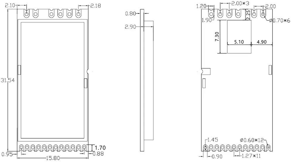
Size:31.54*15.8
★ The following parameters are obtained by connecting the instrument with a 50 ohm copper axis:@VCC=5 V.
| Parameter | Min. | Typ. | Max. | Unit | Condition |
| Operation Condition | |||||
| Working voltage | 2 | 5 | 5.5 | V | |
| Temperature range | -40 | 85 | °C | ||
| Current Consumption | |||||
| TX current | < 600 | mA | @Vcc=5V, 27dBm | ||
| RX current | < 17 | mA | @Ordinary crystal | ||
| Sleep current | <7 | uA | |||
| RF Parameter | |||||
| Frequency range | 2400 | 2500 | MHz | ||
Data rate | 0.476 | 202 | Kbps | @LoRa | |
| 260 | 1300 | Kbps | @FLRC | ||
| 125 | 2000 | Kbps | @FSK | ||
| Output power | 1 | 27 | dBm | ||
| Maximum Output power | 26 | 26.5 | 27 | dBm | @VCC=5V |
| Receiving sensitivity | -132 | dBm | LoRa@0.476kbps | ||
| Interface | SPI |
| Chip | SX1280 |
| Frequency | 2.4GHz |
| Modulation | LoRa |
| Output Power | 500mW |
| Certification | FCC ID, CE-RED |


Note: When the power supply is 5V, the high level of all IO is 3.3V.
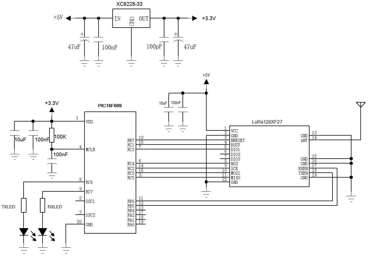
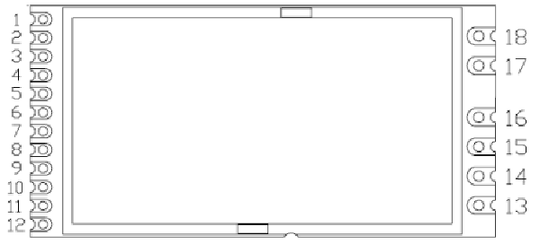
| Pin NO | Pin name | I/O | Level standard | Description |
| 1 | VCC | - | 2.0-5.5V | Connected to the positive pole of the power supply |
| Note: In LoRa1280F27-TCXO module, PIN 2 is TCXOEN | ||||
| 2 | GND | - | Power ground | |
| Note: In LoRa1280F27-TCXO module, PIN 2 is TCXOEN | ||||
2 | TCXOEN | I | 2.0-3.3V | Turn on TCXO: Pull up TCXOEN before controlling SX1280 to reset; Delay at least 3ms to wait for the TCXO startup to complete; 3. During the use of the 1280 module, TCXOEN must always maintain a high level; Turn off TCXO (if the module needs to enter sleep mode): Call the SetSleep() function to make the module enter the sleep mode; Delay at least 1ms to wait for the completion of module sleep; Pull down TCXOEN to turn off TCXO; |
| 3 | NRESET | I | 0-3.3V | Chip reset trigger pin, active low |
4 | BUSY | O | 0-3.3V | Status indicator pin (see SX1280/1281 specification for details) |
5 | DIO1 | O | 0-3.3V | Directly connected to the chip pin, configurable general-purpose IO (see the chip SX1280/1281 specification for details) |
6 | DIO2 | O | 0-3.3V | Directly connected to the chip pin, configurable general-purpose IO (see the chip SX1280/1281 specification for details) |
7 | DIO3 | O | 0-3.3V | Directly connected to the chip pin, configurable general-purpose IO (see the chip SX1280/1281 specification for details) |
| 8 | NSS | I | 0-3.3V | Module chip select pin |
| 9 | SCK | I | 0-3.3V | SPI clock input pin |
| 10 | MOSI | I | 0-3.3V | SPI data input pin |
| 11 | MISO | O | 0-3.3V | SPI data output pin |
| 12,15.16 | GND | - | - | Connected to the negative pole |
13 | TXEN | I | 0-3.3V | Transmission control pin (high level when transmitting, low level when receiving) |
14 | RXEN | I | 0-3.3V | Receive control pin (high level when receiving, low level when transmitting) |
| 17 | ANT | - | - | Connect with 50 ohm coaxial antenna |
| 18 | GND | - | - | Connected to the negative pole |

Privacy Policy
· Privacy Policy
There is currently no content available
Email:sales@nicerf.com
Tel:+86-755-23080616