Contact us
HOME > PRODUCTS > LORA & LORAWAN MODULES (SPI ) > LORA1280F27-TCXO : SX1280 2.4GHZ INDUSTRIAL-GRADE...
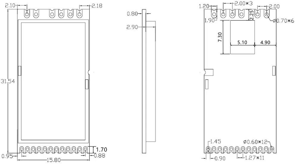
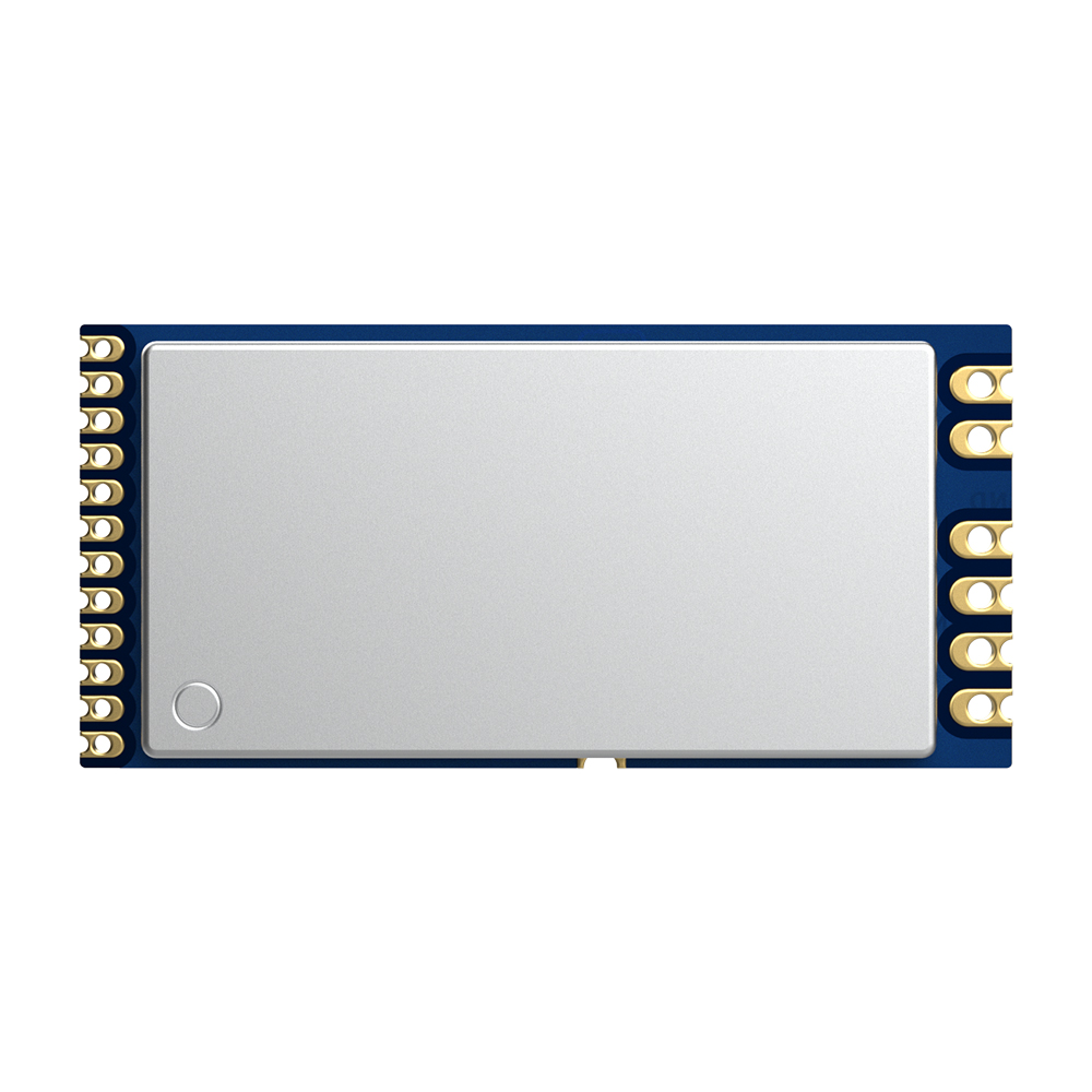
LoRa1280F27-TCXO : SX1280 2.4GHz Industrial-Grade RF Module
- This series of modules are designed based on the original sx1280 RF chip from Semtech,and the matching of the PA circuit makes the output power of the module up to 500mW(+27dBm).In addition, the LoRa1280F27-TCXO module is also equipped with an industrial-grade high-precision TCXO temperature-compensated crystal oscillator, which guarantees stable frequency output under harsh environments such as high and low temperature.
- The 2.4GHz RF Module LoRa1280F27-TCXO strictly uses lead-free process for production and testing, and meets RoHS and Reach standards.
★ The following parameters are obtained by connecting the instrument with a 50 ohm copper axis:@VCC=5 V.
| Parameter | Min. | Typ. | Max. | Unit | Condition |
| Operation Condition | |||||
| Working voltage | 2 | 5 | 5.5 | V | |
| Temperature range | -40 | 85 | °C | ||
| Current Consumption | |||||
| TX current | < 600 | mA | @Vcc=5V, 27dBm | ||
|
RX current | < 17 | mA | @Ordinary crystal | ||
| < 19 | mA | @TCXO | |||
| Sleep current | <7 | uA | |||
| RF Parameter | |||||
| Frequency range | 2400 | 2500 | MHz | ||
|
Data rate | 0.476 | 202 | Kbps | @LoRa | |
| 260 | 1300 | Kbps | @FLRC | ||
| 125 | 2000 | Kbps | @FSK | ||
| Output power | 1 | 27 | dBm | ||
| Maximum Output power | 26 | 26.5 | 27 | dBm | @VCC=5V |
| Receiving sensitivity | -132 | dBm | LoRa@0.476Kbps | ||
| Interface | SPI |
| Chip | SX1280 |
| Frequency | 2.4GHz |
| Modulation | LoRa |
| Output Power | 500mW |
Features of 2.4GHz RF Module LoRa1280F27-TCXO
- Operating frequency range:2400-2500MHz
- Maximum output power:500mW (27.0dBm)
- Sensitivity up to--132dBm@LoRa
- Data transfer rate:@LoRa=0.476-202kPbs
- LoRa modulation
- Built-in LNA
- High precision crystal oscillator (0.5ppm TCXO/10ppm)
- Packet communication mode(receiving FiFo 256 bytes)
- Operating voltage range:2.0-5.5V
- Operating temperature range:-40~+85 °C
Applications of 2.4GHz RF Module LoRa1280F27-TCXO
- Wireless remote
- Smart home
- Tag reader
- Toy control
- Tire pressure monitoring
- Health monitoring


Note: When the power supply is 5V, the high level of all IO is 3.3V.
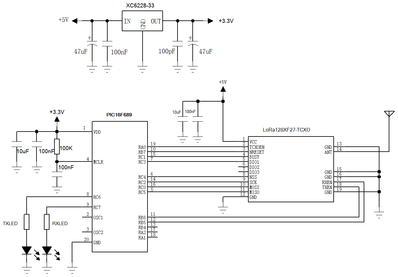
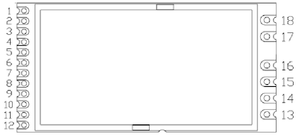
| Pin NO | Pin name | I/O | Level standard | Description |
| 1 | VCC | - | 2.0-5.5v | Connected to the positive pole of the power supply |
| Note: In Lora1280F27-TCXO module, PIN 2 is TCXOEN | ||||
| 2 | GND | - | Power ground | |
| Note: In Lora1280F27-TCXO module, PIN 2 is TCXOEN | ||||
| 2 | TCXOEN | I | 2.0-3.3V | Turn on TCXO: Pull up TCXOEN before controlling SX1280 to reset; Delay at least 3ms to wait for the TCXO startup to complete; 3. During the use of the 1280 module, TCXOEN must always maintain a high level; Turn off TCXO (if the module needs to enter sleep mode): Call the SetSleep() function to make the module enter the sleep mode; Delay at least 1ms to wait for the completion of module sleep; Pull down TCXOEN to turn off TCXO; |
| 3 | NRESET | I | 0-3.3V | Chip reset trigger pin, active low |
| 4 | BUSY | O | 0-3.3V | Status indicator pin (see SX1280/1281 specification for details) |
| 5 | DIO1 | O | 0-3.3V | Directly connected to the chip pin, configurable general-purpose IO (see the chip SX1280/1281 specification for details) |
| 6 | DIO2 | O | 0-3.3V | Directly connected to the chip pin, configurable general-purpose IO (see the chip SX1280/1281 specification for details) |
| 7 | DIO3 | O | 0-3.3V | Directly connected to the chip pin, configurable general-purpose IO (see the chip SX1280/1281 specification for details) |
| 8 | NSS | I | 0-3.3V | Module chip select pin |
| 9 | SCK | I | 0-3.3V | SPI clock input pin |
| 10 | MOSI | I | 0-3.3V | SPI data input pin |
| 11 | MISO | O | 0-3.3V | SPI data output pin |
| 12,15.16 | GND | - | - | Connected to the negative pole |
| 13 | TXEN | I | 0-3.3V | Transmission control pin (high level when transmitting, low level when receiving) |
| 14 | RXEN | I | 0-3.3V | Receive control pin (high level when receiving, low level when transmitting) |
| 17 | ANT | - | - | Connect with 50 ohm coaxial antenna |
| 18 | GND | - | - | Connected to the negative pole |


