SA316S : High Fidelity Wireless Audio Module
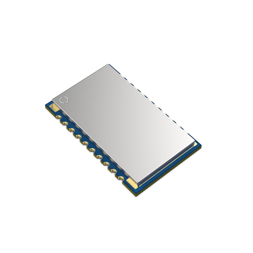
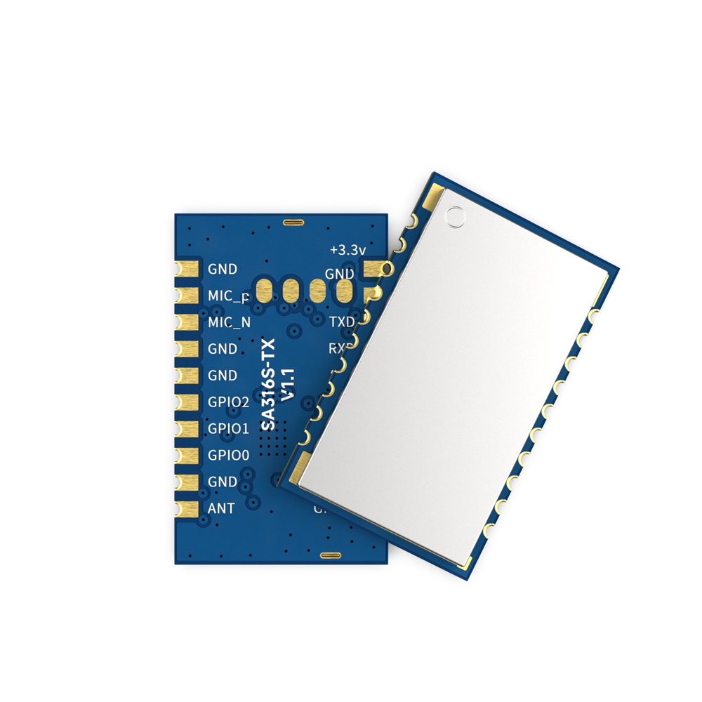
The SA316S series products are divided into transmitter modules SA316S-TX, SA316F30, and receiver module SA316S-RX. This series uses a wireless high-quality voice transmission chip for its design. It can support external PCM / IIS dual-mode digital audio interfaces, and provides customers with a standardized serial interface. Users can quickly and easily set the module's transceiver frequency, volume, microphone gain, and other parameters through serial port commands, which is widely used in situations that require high sound quality.
Parameter | Test Conditions | Min. | Typ. | Max. | Unit |
Operating voltage range | @SA316S-TX, SA316-RX | 2.8 | 3.3 | 3.6 | V |
@SA316F30 | 3.3 | 4.0 | 5.0 | ||
Range of working temperature | -20 | 25 | 60 | ℃ | |
Operating frequency range | @UHF | 500 | 540 | MHz | |
800 | 890 | MHz | |||
890 | 980 | MHz | |||
@VHF | 160 | 270 | MHz | ||
Audio transmission and reception delay | 4 | ms | |||
Serial port baud rate | 9600 | bps | |||
Current consumption | |||||
Sleep current(SA316-RX) | <0.4 | mA | |||
Sleep current (SA316S-TX,SA316F30) | 5 | 10 | uA | ||
Receive current(SA316-RX) | @VCC=3.3V | < 115 | mA | ||
Transmit Current(SA316S-TX) | @ During Transmission | < 100 | mA | ||
@Not Transmitting | <54 | mA | |||
Transmit Current(SA316F30-TX) | @During Transmission,5v | < 700 | mA | ||
@Not Transmitting,5v | <60 | mA | |||
Transmit parameter | |||||
Transmit power | @SA316S-TX, VCC=3.3V | 9 | 10 | 11 | dBm |
@SA316F30-TX, VCC=5.0V | 29 | 30 | 31 | dBm | |
Emission bandwidth(BW) | 300 | KHz | |||
Adjacent channel power ratio(ACPR) | @600KHZ | -60 | dBc | ||
Maximum microphone input voltage | 0.1 | 1.0 | Vrms | ||
Audio frequency response range | 30 | 20k | Hz | ||
Receive parameters | |||||
Receiving sensitivity | -96 | dBm | |||
Audio output amplitude (differential) | 400 | mVrms | |||
Audio output drive resistance | 600 | Ohm | |||
Signal to Noise Ratio (SNR) | @1KHz | 86 | dB | ||
Total harmonic distortion (THD) | @48KSampling Rate | 0.07 | % | ||
| Type | Wireless audio |
| Output Power | 10mW |
Features of SA316 Wireless Audio Module
- UHF frequency band:500MHz/868 MHz915MHz, UHF frequency band:450~980 MHz, VHF frequency band:160~270 MHz
- The transmission distance is 200 meters in the open area
- Receiving sensitivity: -96 dBm
- Audio signal to noise ratio: 86 dB
- Frequency response: 20 Hz-20 KHz
- The delay from microphone input to audio output is less than 3ms
- Digital modulation method: pi/4 DQPSK
- Occupied bandwidth: <300 KHz
- Transmission rate 204.8 Ksps
- Sampling rate: 48 KHz
Applications of SA316 Wireless Audio Module
- Wired speakers become wireless speakers
- wireless microphone
- Wireless Headphones
- High-quality wireless audio transmission
Analog input and analog output application circuit


IIS input and output application circuit


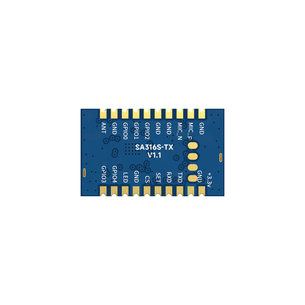
SA316-TX
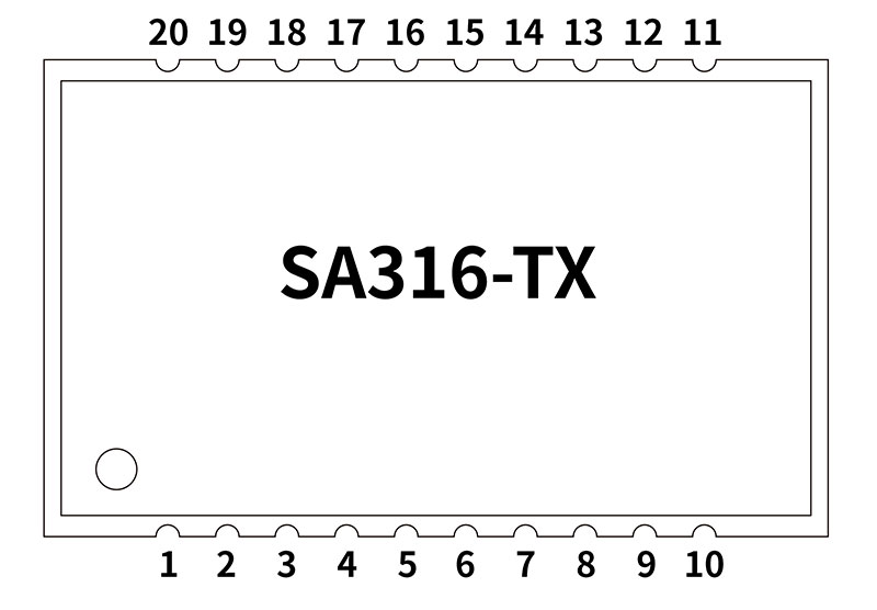
| Pin NO. | Pin name | I/O | Level standard | Description |
| 1 | ANT | 0 | RF signal output, connect to 50 ohm antenna | |
| 2、6、7、10、12、17 | GND | 0V | Connect to the negative pole of the power supply | |
| 3 | GPIO0 | I/O | 0-3.3V | The GPIO0 of the built-in audio chip can be configured as LRCK when using I2S mode |
| 4 | GPIO1 | I/O | 0-3.3V | The GPIO1 of the built-in audio chip can be configured as SCK when using I2S mode |
| 5 | GPIO2 | I/O | 0-3.3V | The GPIO2 of the built-in audio chip can be configured as MCLK when using I2S mode |
| 8 | MIC_N | I | Negative end of microphone input, can be left floating | |
| 9 | MIC_P | I | Positive end of microphone input, (the best signal is less than 300mVrms) | |
| 11 | VCC | +3.3V | Power positive input (2.8V-3.6V, typical 3.3V) | |
| 13 | TXD | O | 0-3.3V | Serial data output |
| 14 | RXD | I | 0-3.3V | Serial data input |
| 15 | SET | I | 0-3.3V | Function temporarily reserved |
| 16 | CS | I | 0-3.3V | Module sleep pin (low level work, high level sleep) |
| 18 | LED | O | 0-3.3V | Output indication, high output when transmitting signal, low output when not transmitting signal |
| 19 | GPIO4 | I/0 | 0-3.3V | GPIO4 of the built-in audio chip |
| 20 | GPIO3 | I/O | 0-3.3V | The GPIO3 of the built-in audio chip can be configured as SDIN when using I2S mode |
SA316-RX
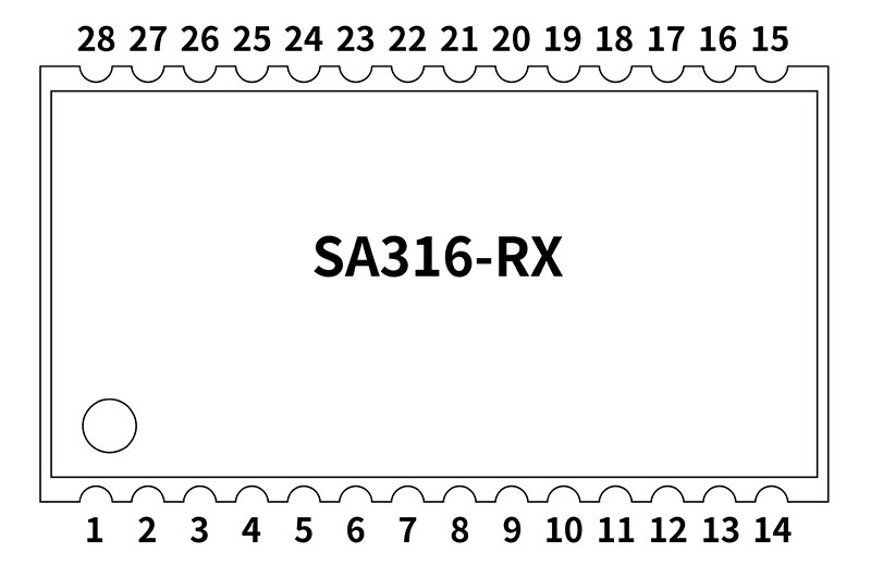
| Pin NO. | Pin name | I/O | Level standard | Description |
| 1 | VCC | +3.3V | Power positive input (2.8V-3.6V, typical 3.3V) | |
| 2,7,9,13,16, 19,21,23,25,27 | GND | 0V | Connect to the negative pole of the power supply | |
| 3 | TXD | O | 0-3.3V | Serial data output |
| 4 | RXD | I | 0-3.3V | Serial data input |
| 5 | SET | I | 0-3.3V | Function temporarily reserved |
| 6 | CS | I | 0-3.3V | Module sleep pin (low level work, high level sleep) |
| 8 | LED | O | 0-3.3V | Output indication, output high after receiving signal, low when no signal |
| 10 | GPIO4 | I/0 | 0-3.3V | GPIO4 of the built-in audio chip |
| 11 | GPIO3 | I/O | 0-3.3V | The GPIO3 of the built-in audio chip can be configured as MCLK when using I2S mode |
| 12 | GPIO2 | I/O | 0-3.3V | The GPIO2 of the built-in audio chip can be configured as SDIO when using I2S mode |
| 15 | ANT | I | RF signal input, connect to 50 ohm antenna | |
| 17 | GPIO1 | I/O | 0-3.3V | The GPIO1 of the built-in audio chip can be configured as SCK when using I2S mode |
| 18 | GPIO0 | I/O | 0-3.3V | The GPIO0 of the built-in audio chip can be configured as LRCK when using I2S mode |
| 20 | AOL+ | O | Chip audio output negative terminal (up to 600mVrms) | |
| 22 | AOR+ | 0 | Chip audio output positive terminal (up to 600mVrms) | |
| 24 | LOUL LOUT+ | O | The amplified audio output is the left channel output, which can directly drive headphones after connecting 100UF capacitors in series | |
| 26 | ROUT+ | O | The amplified audio output is the right channel output, which can directly drive the headphones after connecting a 100UF capacitor in series | |
| 28 | VOL_ADJ | I | Volume adjustment pin, external 50K ohm adjustable potentiometer |
SA316-TX

SA316-RX

SA316F30-TX


 English


