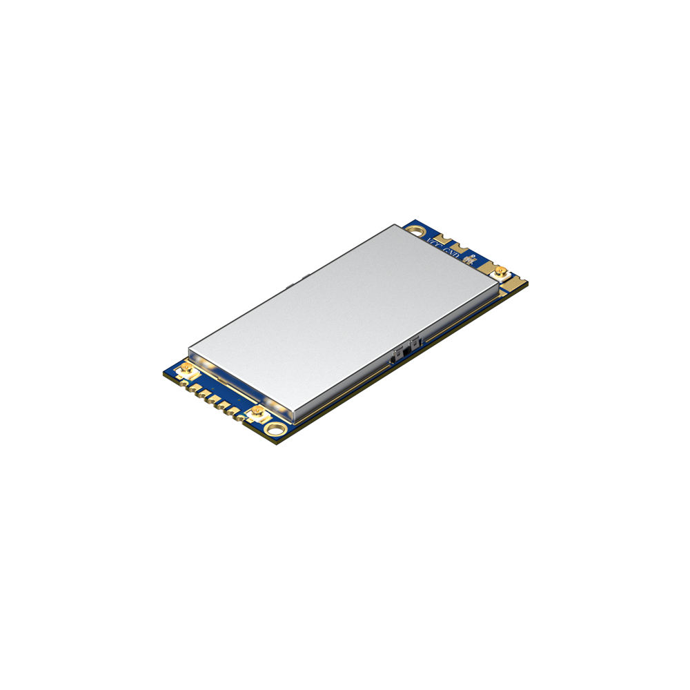
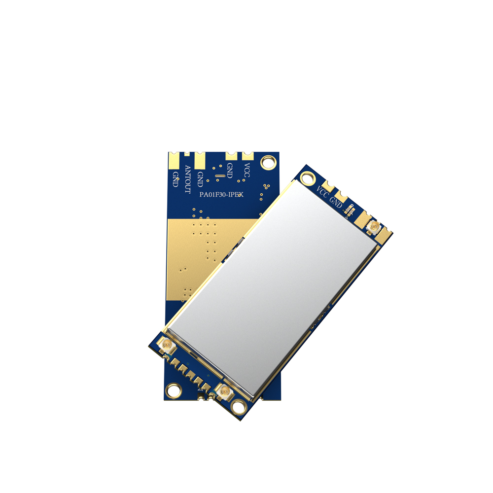
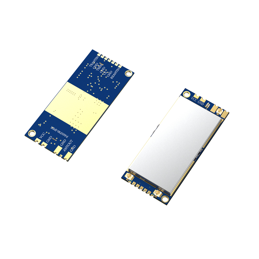
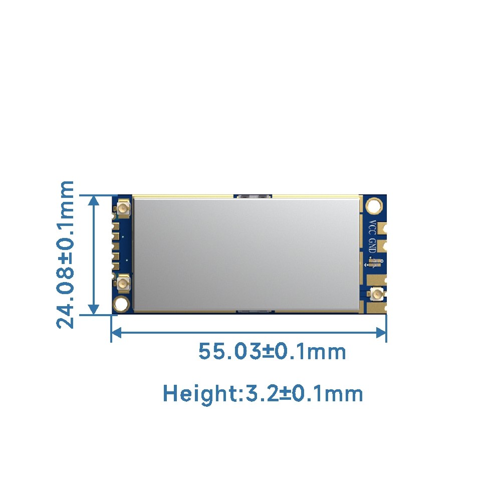
PA01F39: 8V-Powered Low-Noise FEM Power Amplifier Module
PA01F39 module is a high-performance FEM module with an operating frequency range of 400-480 MHz, integrating multiple RF functions. The module has a built-in power amplifier (PA) that supports an input power of up to 30 dBm and an output power of over 39 dBm. It also includes a low-noise amplifier (LNA) and an antenna switch. With its stamp-hole package design, the module is compact and easy to integrate, significantly reducing the difficulty of developing high-power wireless modules and simplifying the design process, thereby enhancing development efficiency.
Parameters | Condition | Min. | Typ. | Max. | Unit |
Power Supply | 4 | 8.5 | V | ||
Working temperature | -40 | 25 | 70 | ℃ | |
Maximum transmit input | 32 | dBm | |||
Maximum receive input | 0 | dBm | |||
Current consumption | |||||
Sleep current | <30 | uA | |||
RX Current | <18 | mA | |||
TX current(High power) | Peak | 2.7 | A | ||
@440MHZ,39dBm,8V,0.5 Duty Cycle | 1.3 | A | |||
RF Parameters | |||||
Operating frequency | 400 | 480 | MHz | ||
Transmit power | @440MHz,TXANTIN 30dBm,Vcc=8v | 38 | 39 | 40 | dBm |
Receiver low-noise gain | @400-480MHz Input -50dBm | 10 | 20 | dB | |
Receiver noise figure | 1.0 | dB | |||
Features
Ultra-wide frequency range: 400-480 MHz
Wide voltage range: 4-8.5V
Built-in transmit/receive switch, allowing both reception and transmission with a single antenna
Built-in low-noise amplification, with a noise figure (NF) of 1.0 dB
Applications
High-power amplification for wireless data transmission
High-power amplification for wireless voice transmission

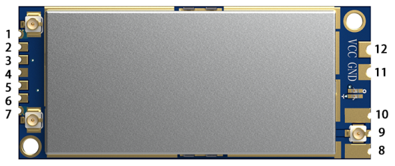
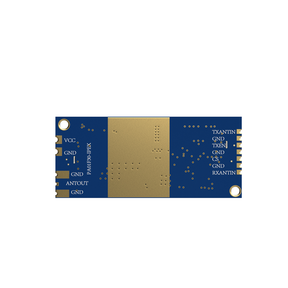
Pin NO | Pin name | I/O | Description |
1 | TXANTIN | - | The amplifier signal input pin should not exceed a maximum input signal of 32dBm |
2,4,6,8,10,11 | GND | - | Connect to power ground |
3 | TXEN | 0-3.3V | Transmit enable control pin,High level for transmission, low level for reception. (Note: This pin also controls the gate voltage of the internal power amplifier. The high level should not exceed 3.3V, as higher voltage may damage the internal power amplifier IC.) |
5 | CS | 0-5v | Sleep pin,This pin should be pulled high during operation and pulled low during sleep. There is no internal pull-up. |
7 | RXANTOUT | - | Receiver signal output pin,Connect to the external matching circuit of the user's product. If the user only intends to use it for power amplification, this pin can remain unconnected. |
9 | ANTOUT | - | Power amplifier output pin and receiver signal input pin |
12 | VCC | 0-8.5V | Module power supply positive input |


 English


