2.4 GHz transmitter and receiver module schematic analysis
When we purchase a 2.4 GHz transmitter and receiver module, the best way to understand its performance principle is to look at the internal schematic diagram of the module. It can help us understand the performance principle of the module faster and more clearly. Considering that many users or friends who have just entered the Internet of Things do not know the internal schematic diagram very well, today NiceRF takes the 2.4 GHz transmitter and receiver module RF2401F27 as an example to explain how the internal schematic diagram of the 2.4 GHz wireless module is analyzed.
2.4 GHz transmitter and receiver module schematic analysis

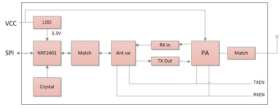
(Internal schematic of 2.4 GHz transmitter and receiver module RF2401F27)
The first step: we must first understand that the 2.4 GHz transmitter and receiver module RF2401F27 is composed of those circuit components:
LDO: Step-down circuit, the function is to input a stable voltage value within the input range.。
nRF24L01+:Core chip, the most important IC chip of the entire RF2401F27 module。
Crystal: The main function is to generate frequency。
Match:Matching circuit
PA:It is the power amplifier we often say. I have written about how to amplify the power of the wireless module. This PA is one of the ways.
Ant sw:Antenna switch
RX in:Receiving circuit
TX Out:Transmitting circuit
TXEN、RXEN:Enable pin for controlling Ant sw (antenna switch)
VCC:power input
SPI:Level interface
As shown in the figure, when the nRF24L01+ chip outputs a signal, it first goes through the transmitting matching circuit and then goes to the circuit antenna switch, then goes through the PA amplifier circuit to amplify the signal, and finally goes through the antenna matching circuit and outputs it to the antenna, where it is radiated by the antenna. This is a complete transmission process of the 2.4 GHz transmitter and receiver module RF2401F27.
Transmitting process: Since the 2.4 GHz transmitter and receiver module RF2401F27 does not need to pass the PA power amplifier when receiving signals, when the signal is received by the antenna, it first passes through the matching circuit of the antenna, then goes to the RX In receiving circuit to the Ant sw antenna switch, and finally enters the Match matching circuit. Enter the nRF24L01+ chip。
Today's 2.4 GHz transmitter and receiver module is resolved to this. Do you understand the parsing process of this schematic? If you still have any questions or need to know other questions, please feel free to contact NiceRF.
 +86-755-23080616
 sales@nicerf.com
Website: https://www.nicerf.com/
Address: 309-314, 3/F, Bldg A, Hongdu business building, Zone 43, Baoan Dist, Shenzhen, China


