Contact us
HOME > PRODUCTS > BLUETOOTH MODULES > BLE5201 : BLE 5.2 SILABS CORE CHIP
BLE5201 : BLE 5.2 Silabs Core Chip
- The company's BLE5201 BLE module uses BLE 5.2 protocol and uses Silicon Labs' EFR32BG22C224 SOC chip. It has the characteristics of low power consumption, small size, long transmission distance, and strong anti-interference ability.
- BLE5201 has ultra-low transmitting and receiving current (3.6 mA when transmitting power is 0 dBm; receiving 2.6 mA) and high-performance, low-power M33 core, which can extend the life of button batteries to ten years. Target applications include Bluetooth Mesh low-power nodes, smart door locks, personal healthcare and fitness equipment. The SOC’s Bluetooth Angle of Arrival (AoA) and Angle of Departure (AoD) functions and positioning accuracy within 1 meter will also benefit applications such as asset tracking tags, beacons, and indoor navigation. EFR32BG22C224 SOC provides IQ sampling capability, suitable for direction finding applications, and supports 125 KB and 500 KB Bluetooth Low Energy Coded PHY, which can increase the receiving sensitivity to -106 dBm. Supports applications that require direction finding or low energy Bluetooth Mesh nodes.
- BLE5201 BLE module strictly uses lead-free technology for production and testing, and meets RoHS and Reach standards.
| Parameter | Performance | Remark | |||
| Min. | Typ. | Max. | |||
| Operating Voltage(V) | 1.8 | 3.3 | 4.3 | >= 3.3V guaranteed output power | |
| Communication level(V) | 3.3 | ||||
| Operating temperature(℃) | -40 | 85 | Industrial design | ||
| Working frequency(MHz) | 2400 | 2483.5 | |||
| Transmit power(dBm) | 0 | 6 | |||
| Receiving sensitivity(dBm) | -94.6 | ||||
| Power consumption | Emission current(mA) | 7.5 | |||
| Receive current(mA) | 8.5 | ||||
| Sleep current(uA) | < 5 | When there is no connection | |||
| Idle state current(mA) | 6.58 | Idle state: refers to no connection, no broadcasting/scanning of the module | |||
| Type | Bluetooth |
Features of BLE module BLE5201
- Developed based on Bluetooth BLE5.2 protocol
- Support single slave and one master with multiple slaves, can connect multiple slaves at the same time, up to 8 connections
- Support 2 working modes of configuration and transparent transmission
- Support over-the-air upgrade (OTA DFU)
- Support low power sleep
- Support automatic broadcasting, scanning, connection
- Support manual connection and automatic connection 2 connection methods
- The maximum MTU is 247 bytes
- Support custom 16-bit UUID, including one Service UUID and two Characteristic UUID
- Maximum transmission distance 150m (6dBm, Coded PHY)
- Support automatic binding
- Support multiple serial port parameter configuration
Applications of BLE module BLE5201
- Wireless meter reading wireless sensor
- Smart home
- Industrial remote control, telemetry
- Smart buildings, smart buildings
- Automated data collection
- Health sensor
- Smart wearable device
- Smart robot
- Wireless sensing
- Electronic tags
- Intelligent control


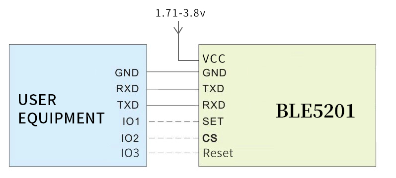
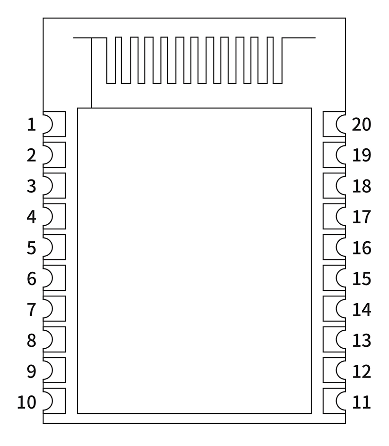
| Pin NO. | Pin name | Pin direction | Pin function | Description |
| 1 | GND | Enter | Power ground | |
| 2 | PA00 | Enter | Disconnect pin | Pull up by default. Low level: disconnect all Bluetooth connections and stop broadcasting/scanning; high level: resume broadcasting/scanning |
| 3 | PA01 | SWCLK | ||
| 4 | PA02 | SWDIO | ||
| 5 | PA03 | Enter | Wake-up pin CS | Default pull-up: low level work, high level sleep |
| 6 | PA04 | Enter | Module selection SET | Pull up by default. High level: transparent transmission mode; low level: configuration mode |
| 7 | PA05 | TXD | Module serial data sending pin | |
| 8 | PA06 | RXD | Module serial port data receiving pin | |
| 9 | GND | Power ground | ||
| 10 | VCC | Power positive | ||
| 11 | PC00 | GPIO | ||
| 12 | PC01 | GPIO | ||
| 13 | PC02 | GPIO | ||
| 14 | PC03 | GPIO | ||
| 15 | PC04 | GPIO | ||
| 16 | PC05 | GPIO | ||
| 17 | PB02 | Output | Sleep state | Wake-up mode: high level; low power consumption mode: low level |
| 18 | PB01 | Output | Mode status | Transparent transmission mode: low level; configuration mode: high level |
| 19 | RESET | Output | Reset | Built-in pull-up resistor, active low |
| 20 | PB00 | Output | Connection Status | With connection: high level; no connection: low level |


