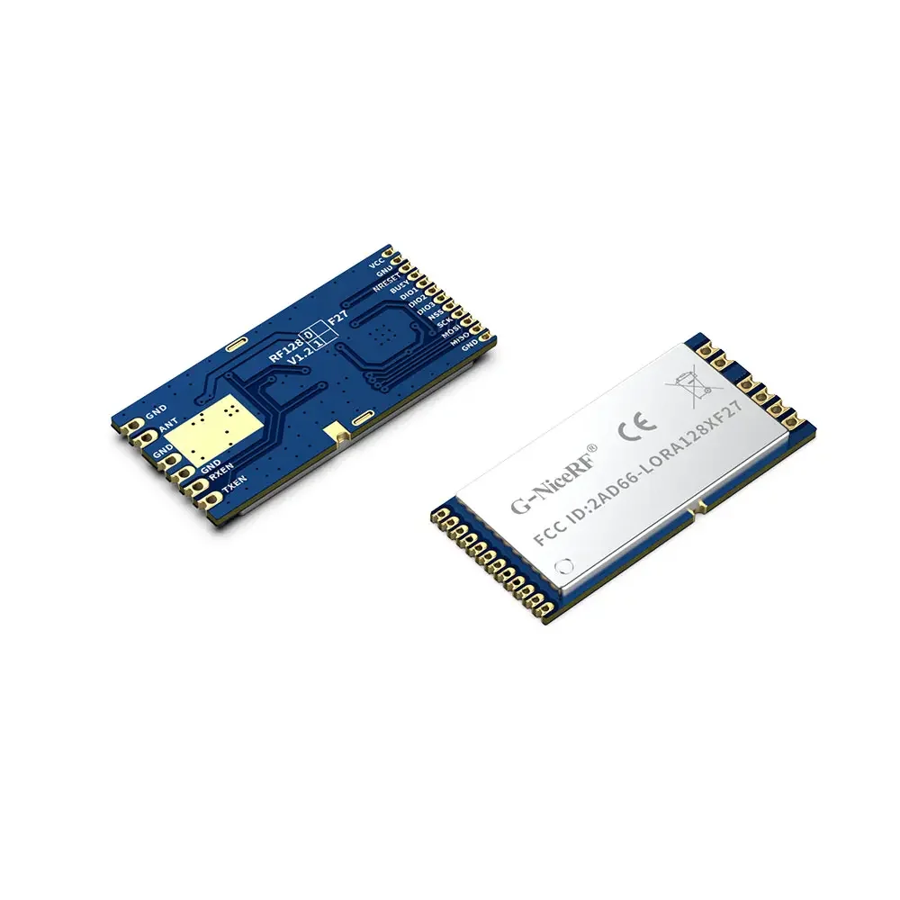
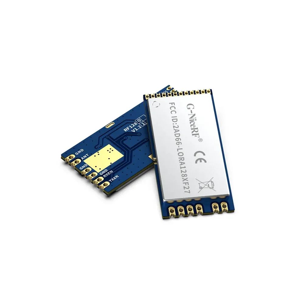


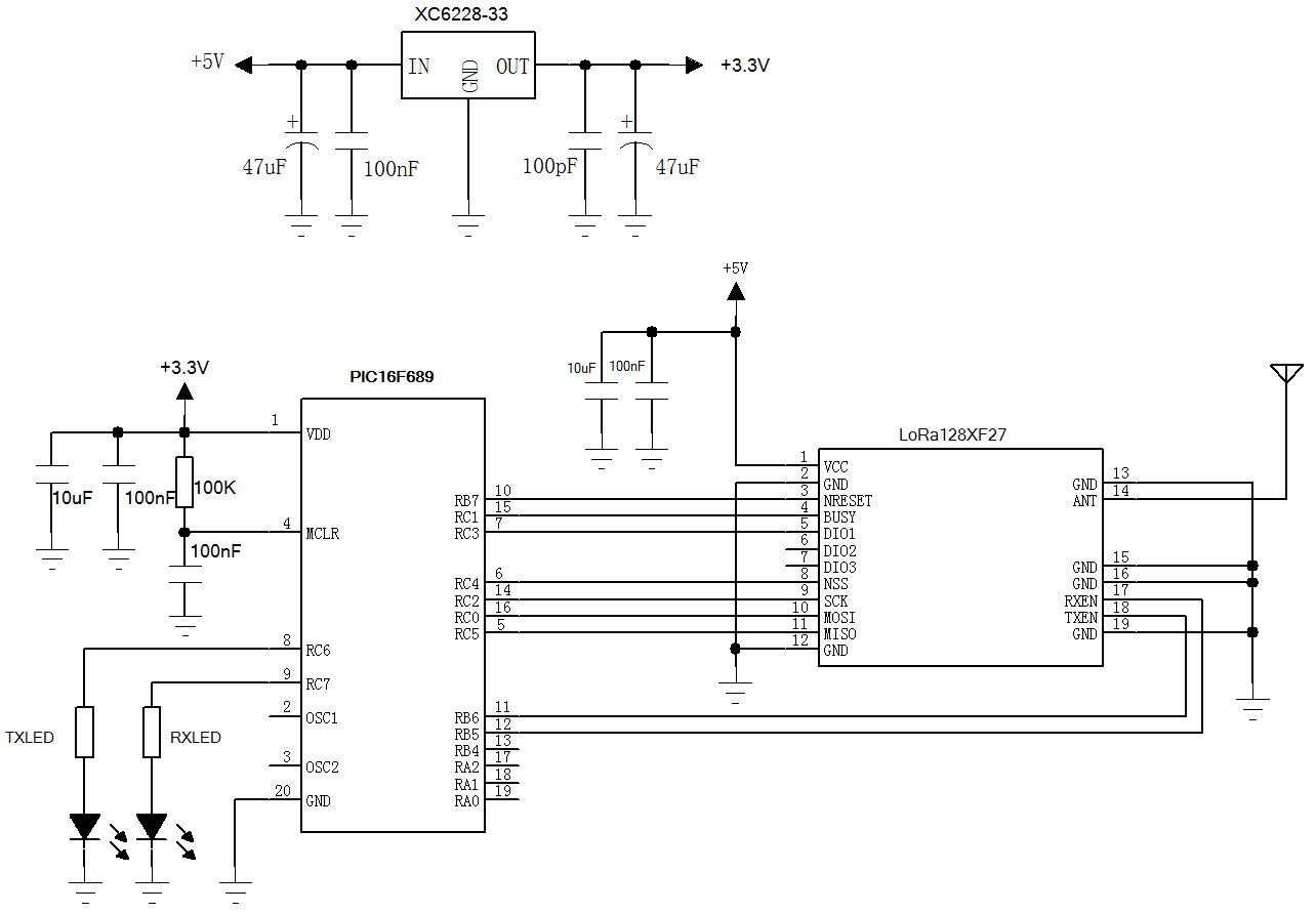
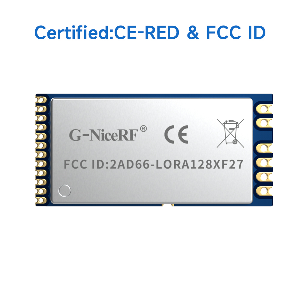
LoRa1280F27 : SX1280 500mW FCC ID & CE-RED Certified 2.4GHz LoRa Module With SPI Interface Power
Type: LoRa Front-End Modules
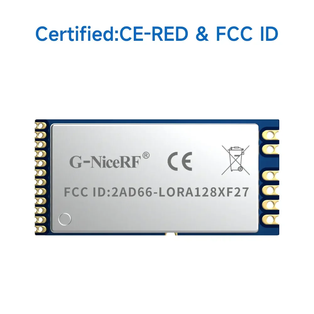
Certification: CE-RED,FCC ID
Modulation: LoRa
Chip: SX1280
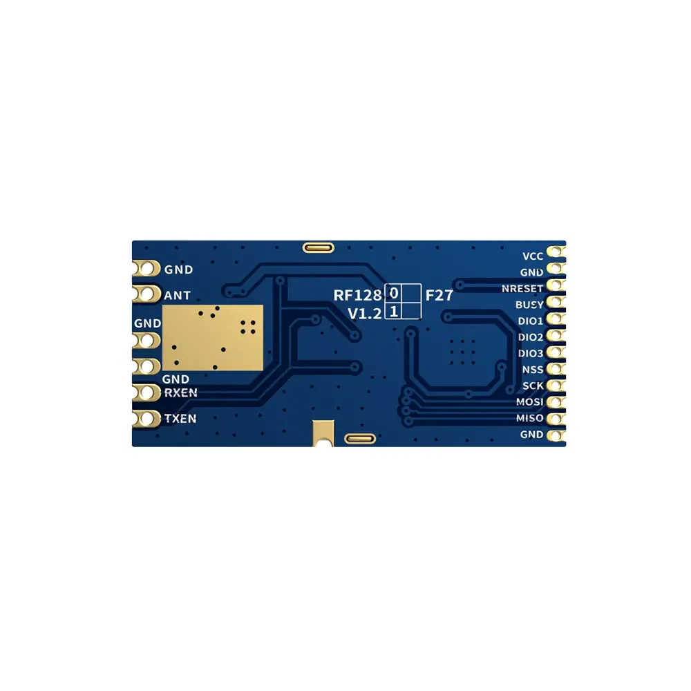
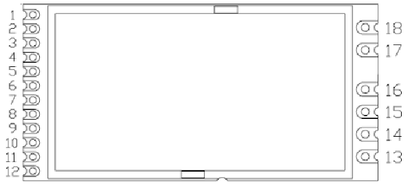
Interface: SPI
Output Power: 500mW
Frequency: 2.4GHz
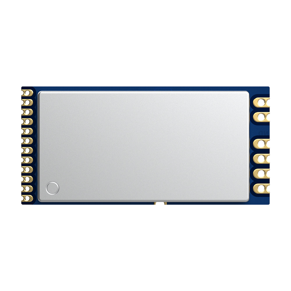
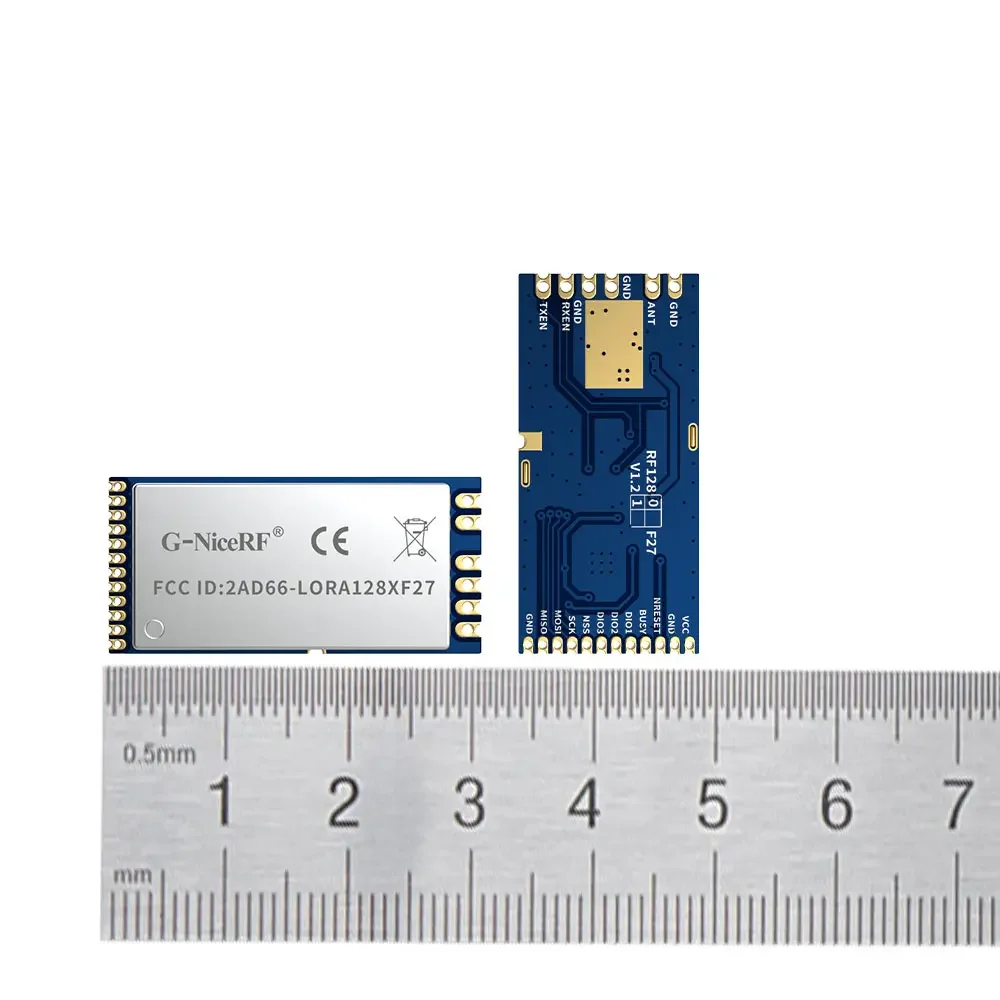
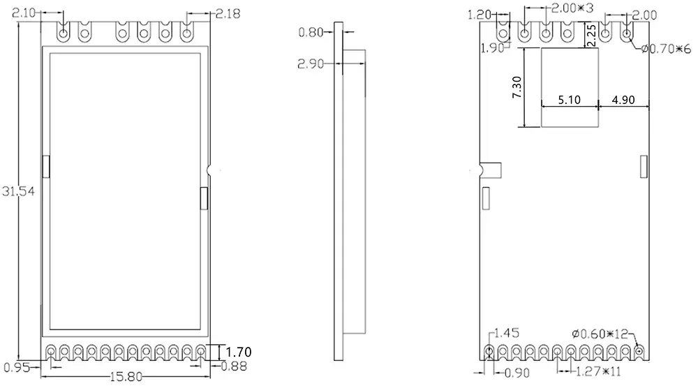
Size:31.54*15.8