

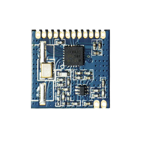
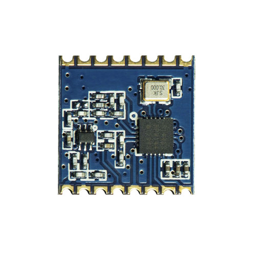
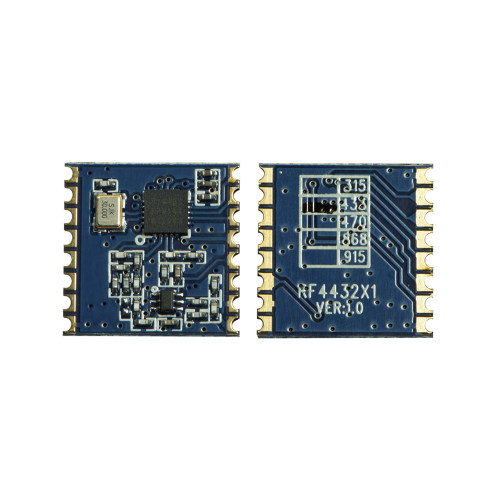
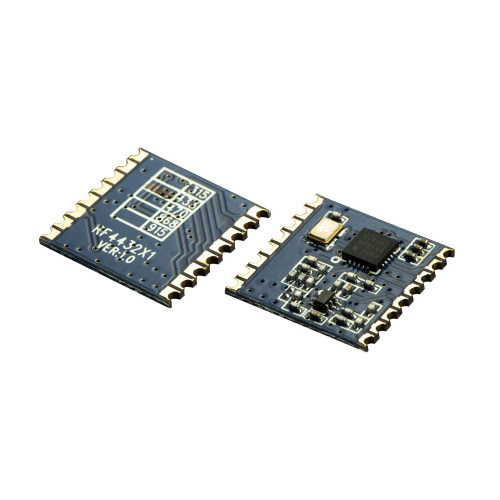
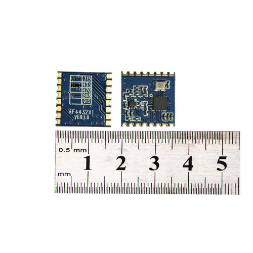
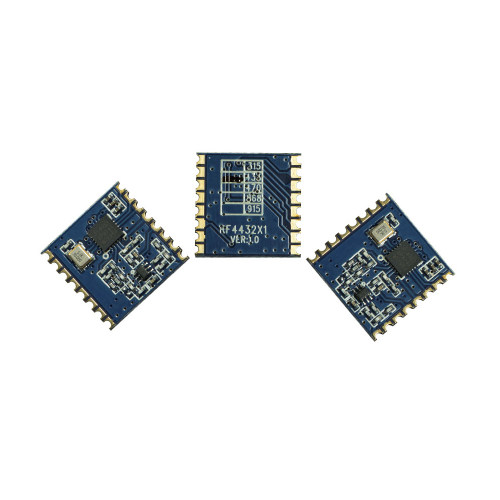
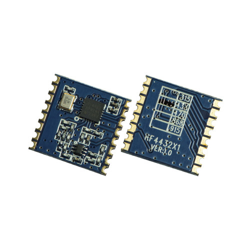
RF4432 : 100mW Si4432 RF Transceiver Module With Front End Module
Certification: Others
Modulation: (G)FSK
Chip: si4432
Interfacce: SPI
Output Power: 100mW
Frequency: 315MHz,433MHz,470MHz,868MHz,915MHz
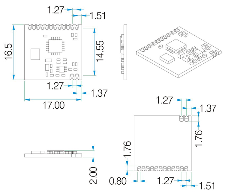
Size:16.5*17
| Parameter | Min | Typ. | Max. | Unit | Condition |
| Operation Condition | |||||
| Working voltage range | 1.8 | 3.3 | 3.6 | V | |
| Temperature voltage | -40 | 85 | ℃ | ||
| Current Consumption | |||||
| RX current | 18.5 | mA | |||
| TX current | 85 | mA | @20dBm | ||
| Sleep current | < 1 | uA | |||
| RF Parameter | |||||
| Frequency range | 403 | 433 | 463 | MHz | @433MHz |
| 470 | 490 | 510 | MHz | @490MHz | |
| 838 | 868 | 898 | MHz | @868MHz | |
| 900 | 915 | 930 | MHz | @915MHz | |
| Modulation rate | 0.123 | 256 | Kbps | FSK | |
| Output power range | 1 | 20 | dBm | ||
| Receiving sensitivity | -121 | dBm | @Data rate=1.2Kbps | ||
| Modulation | (G)FSK |
| Chip | si4432 |
| Frequency | 315MHz,433MHz,470MHz,868MHz,915MHz |
| Output Power | 100mW |
| Interface | SPI |
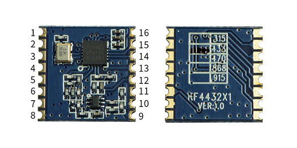
| Pin NO. | Pin Name | Description |
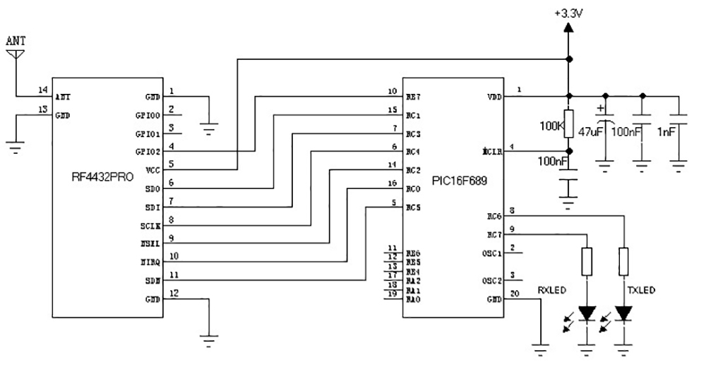
| 1 | ANT | Connect with 50 ohm coaxial antenna |
| 2 | GND | Power ground |
| 3 | RX_ANT | Transmit antenna switch control pin |
| 4 | TX_ANT | Receiving antenna switch control pin |
| 5 | VCC | Connect to the positive power supply 3.3V |
| 6 | GPIO0 | Connect directly to the GPIO0 pin of the chip |
| 7 | GPIO1 | Connect directly to the GPIO1 pin of the chi |
| 8 | GPIO2 | Connect directly to the GPIO 2 pin of the chi |
| 9 | GND | Power ground |
| 10 | SDO | 0~VDD V digital output, provides serial readback function to internal control register |
| 11 | SDI | Serial data input. 0~VDD V digital input. This pin is a 4-wire serial data serial data stream bus. |
| 12 | SCLK | Serial clock input. 0~VDD V digital input. This pin provides a 4-wire serial data clock function. |
| 13 | NSEL | Serial interface select input pin. 0~VDD V digital input. This pin provides select/enable function for 4-wire serial data bus. This signal is also used to indicate burst read/write mode. |
| 14 | nIRQ | Interrupt output pin |
| 15 | SDN | Chip enable pin. 0~VDD V digital input. SDN=0 in all modes except shutdown mode. When SDN=1, the chip will be completely shut down and the contents of the register will be lost. |
| 16 | GND | Power ground |
Privacy Policy
· Privacy Policy
There is currently no content available
Email:sales@nicerf.com
Tel:+86-755-23080616